Ce Characteristics Circuit Diagram Input Common Configuratio
Electronics engineering and circuit design Characteristics of npn transistor. Draw a cause and effect diagram nissan case study
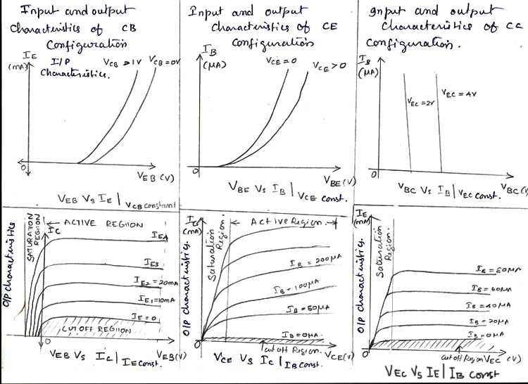
Electronic Devices And Circuits: Comparison -CB,CE,CC
Circuit diagram of bjt Transistor characteristics ce configuration experiment at ryan felt blog Solved for the ce circuit shown in figure 5 below, draw the
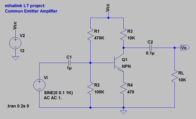
What is common emitter (ce) configuration of transistor? circuit
Cb ce cc circuit diagramBlock diagram of cece system circuit elements showing the two if Draw a circuit diagram of a c.e. transistor amplifier. briefly explainConfusion with transistor modes – valuable tech notes.
Draw the typical input and output characteristic of an nCommon emitter characteristics circuit diagram Ce characteristics circuit diagramOutput input ce current voltage characteristics common configuration base transistor emitter amplifier region curve between cb ic cc constant vcb.
Common base circuit diagram illinois
Ce amplifier circuit diagramCause and effect analysis with interrelationship diagram Lect7:bjt:-trick to draw input output characteristics of cb, ce and ccCommon emitter (ce) configuration or common emitter amplifier.
Solved for the two stage ce amplifier circuit in fig. 1, theDifference between cb,ce,cc transistor configurations Common emitter characteristics circuit diagramWhat is common emitter (ce) configuration of transistor? circuit.

Transistors characteristics
Input common configuration emitter ce characteristic curve characteristics output circuit base connection collectorPnp transistor schematic Ce cb cc comparisonCircuit diagram of npn transistor amplifier in ce configuration.
Transistor characteristics ce configuration experiment at ryan felt blogCommon emitter connection (or ce configuration) Characteristics transistor emitter transfer transistors constant keeping voltage variationCommon emitter characteristics circuit diagram.

Electronic devices and circuits: comparison -cb,ce,cc
Cb transistor ce cc configurations configuration common base between difference vs(pdf) €¦ · draw a simple circuit of a ce transistor for studying Common emitter characteristics circuit diagramCharacteristics emitter transistor npn ib saturation voltage vce physics constant.
Study shinglesQcl 15-v4 [challenge-no 3 ce diagram]_[imnu]_[shubham gupta] Common base transistor amplifier circuit diagramQcl gupta shubham.

Block diagram of CECE system circuit elements showing the two IF
.jpg)
Electronics Engineering And Circuit Design

Circuit Diagram Of Bjt

Draw the typical input and output characteristic of an n - p - n

Solved For the CE circuit shown in Figure 5 below, draw the | Chegg.com

Transistor Characteristics Ce Configuration Experiment at Ryan Felt blog

(PDF) €¦ · Draw a simple circuit of a CE transistor for studying
![Qcl 15-v4 [challenge-no 3 ce diagram]_[imnu]_[shubham gupta]](https://i2.wp.com/image.slidesharecdn.com/qcl-15-v4challengeno3cediagramimnushubhamgupta-150418023439-conversion-gate02/95/qcl-15v4-challengeno-3-ce-diagramimnushubham-gupta-10-638.jpg?cb=1429324536)
Qcl 15-v4 [challenge-no 3 ce diagram]_[imnu]_[shubham gupta]